The Business Research Company’s Semiconductor Metrology And Inspection Market Report 2026 – Market Size, Trends, And Global Forecast 2026-2035
LONDON, GREATER LONDON, UNITED KINGDOM, April 25, 2026 /EINPresswire.com/ — “Semiconductor Metrology And Inspection market to surpass $12 billion in 2030. In comparison, the Navigational, Measuring, Electro medical And Control Instruments market, which is considered as its parent market, is expected to be approximately $1,041 billion by 2030, with Semiconductor Metrology And Inspection to represent around 1% of the parent market. Within the broader Electrical And Electronics industry, which is expected to be $5,611 billion by 2030, the Semiconductor Metrology And Inspection market is estimated to account for nearly 0.2% of the total market value.
Which Will Be The Biggest Region In The Semiconductor Metrology And Inspection Market In 2030?
Asia-Pacific will be the largest region in the semiconductor metrology and inspection market in 2030, valued at $7 billion. The market is expected to grow from $5 billion in 2025 at a compound annual growth rate (CAGR) of 7%. The strong growth can be attributed to rapid expansion of semiconductor fabrication capacity across Asia-Pacific, increasing investments in advanced process control technologies, rising demand for high-precision metrology solutions for advanced nodes, strong presence of leading foundries and integrated device manufacturers, and growing focus on yield optimization and manufacturing efficiency across countries such as China, Taiwan, South Korea, and Japan.
Which Will Be The Largest Country In The Global Semiconductor Metrology And Inspection Market In 2030?
Taiwan will be the largest country in the semiconductor metrology and inspection market in 2030, valued at $2 billion. The market is expected to grow from $1.7 billion in 2025 at a compound annual growth rate (CAGR) of 7%. The strong growth can be attributed to Taiwan’s dominant semiconductor manufacturing ecosystem, high concentration of advanced fabrication facilities, continuous investments in leading-edge process technologies such as 5 nm and 3 nm, increasing demand for precision metrology tools to manage device complexity, and strong collaboration between foundries, equipment manufacturers, and technology providers.
Request A Free Sample Of The Semiconductor Metrology And Inspection Market Report
https://www.thebusinessresearchcompany.com/sample_request?id=8529&type=smp&utm_source=EINPresswire&utm_medium=Paid&utm_campaign=Apr_PR
What Will Be The Largest Segment In The Semiconductor Metrology And Inspection Market In 2030?
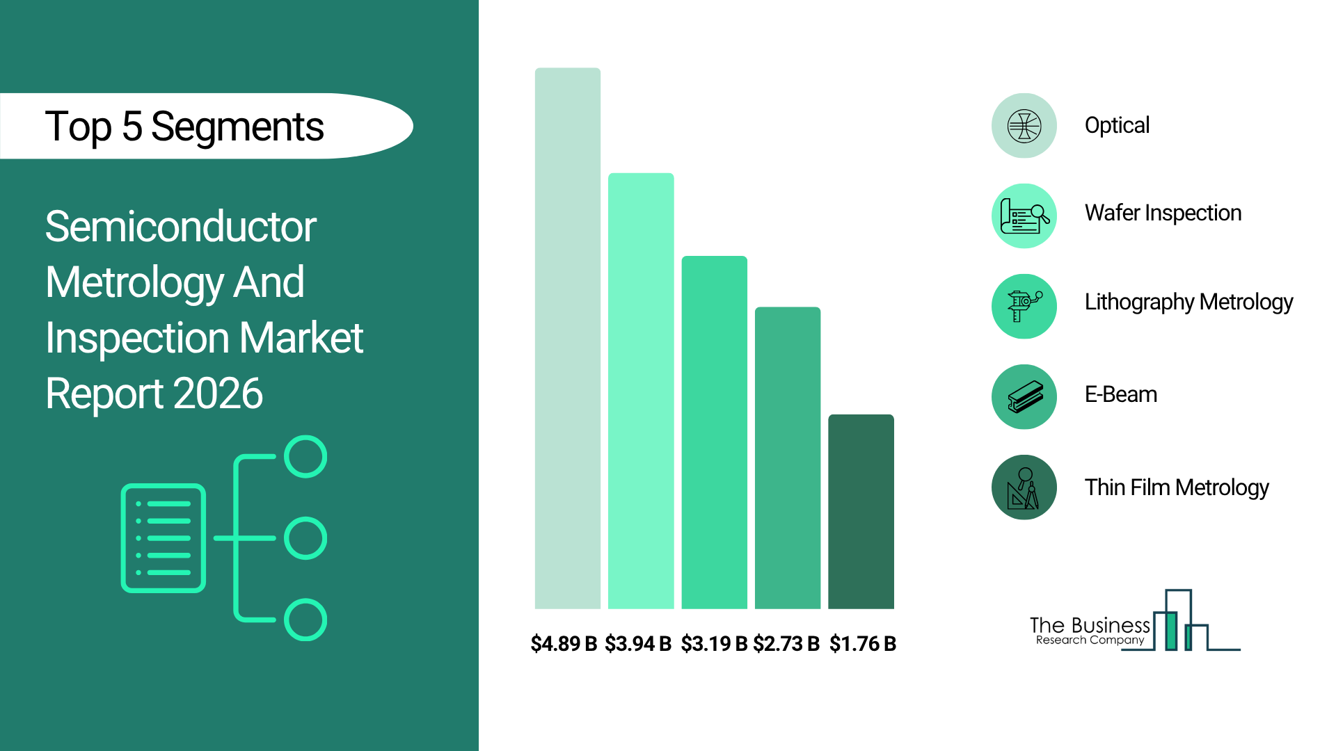
The semiconductor metrology and inspection market is segmented by type into optical, e-beam, and other types. The optical market will be the largest segment of the semiconductor metrology and inspection market segmented by type, accounting for 54% or $6 billion of the total in 2030. The growth of the optical market will be supported by the increasing demand for high-throughput, non-destructive inspection technologies in advanced semiconductor fabrication, rising adoption of optical critical dimension (OCD) and scatterometry techniques for precise process control, and expanding use in monitoring wafer defects across advanced nodes such as 7 nm and below. Additionally, the growing complexity of multi-layer chip architectures, increasing production of logic and memory devices, and continuous upgrades in lithography and wafer fabrication processes are accelerating the adoption of advanced optical metrology and inspection systems across semiconductor manufacturing facilities.
The semiconductor metrology and inspection market is segmented by lithography metrology into overlay, dimension equipment, and mask inspection and metrology. The dimension equipment market will be the largest segment of the semiconductor metrology and inspection market segmented by lithography metrology, accounting for 16% or $2 billion of the total in 2030. The growth of the dimension equipment market will be supported by the increasing need for precise critical dimension (CD) measurement in advanced semiconductor nodes, rising adoption of advanced lithography technologies such as EUV, and the growing complexity of multi-layer chip architectures.
The semiconductor metrology and inspection market is segmented by application into lithography metrology, wafer inspection, and thin film metrology. The wafer inspection market will be the largest segment of the semiconductor metrology and inspection market, segmented by application, accounting for 44% or $5 billion of the total in 2030. The wafer inspection market will be supported by increasing need for early defect detection, rising complexity of semiconductor architectures, growing adoption of high-resolution inspection systems, and increasing focus on yield improvement and process reliability in advanced manufacturing environments.
What Is The Expected CAGR For The Semiconductor Metrology And Inspection Market Leading Up To 2030?
The expected CAGR for the semiconductor metrology and inspection market leading up to 2030 is 7%.
What Will Be The Growth Driving Factors In The Global Semiconductor Metrology And Inspection Market In The Forecast Period?
The rapid growth of the global semiconductor metrology and inspection market leading up to 2030 will be driven by the following key factors that are expected to reshape semiconductor manufacturing process control, advanced node fabrication capabilities, wafer defect detection technologies, yield management strategies, and innovation across global semiconductor equipment and chip production ecosystems.
Increasing Demand For Advanced Node Semiconductor Manufacturing – The increasing demand for advanced node semiconductor manufacturing continues to significantly support the expansion of the semiconductor metrology and inspection market by 2030. The transition toward advanced semiconductor nodes such as 7nm, 5nm, and 3nm requires extremely precise process control and defect detection. Metrology and inspection tools such as CD-SEM and optical overlay measurement are essential for maintaining accuracy in patterning and etching at nanometer scale. As device architectures become smaller and more complex, semiconductor fabs increasingly invest in advanced inspection technologies to maintain yield and performance. As a result, the increasing demand for advanced node semiconductor manufacturing is anticipated to contribute approximately 2.8% annual growth to the market.
Integration Of Artificial Intelligence And Machine Learning In Inspection Systems – The integration of artificial intelligence and machine learning in inspection systems are expected to emerge as a major factor driving the expansion of the semiconductor metrology and inspection market by 2030. The integration of AI and machine learning algorithms into metrology platforms improves defect detection, classification, and predictive maintenance capabilities. These technologies enable automated data analysis, faster process adjustments, and reduced human error in semiconductor manufacturing. AI-enabled inspection tools also improve yield management and process optimization, making them increasingly attractive for advanced semiconductor fabs. Consequently, integration of artificial intelligence and machine learning in inspection systems are projected to contribute around 2.5% annual growth to the market.
Rising Adoption Of In-Line Metrology For Real-Time Process Monitoring – The rising adoption of in-line metrology for real-time process monitoring is expected to act as a key growth catalyst for the semiconductor metrology and inspection market by 2030. Semiconductor manufacturers are shifting from offline quality checks to in-line metrology systems that monitor wafers directly during production. These systems allow real-time identification of process deviations, enabling faster corrective actions and reducing manufacturing defects. The adoption of in-line inspection also improves production efficiency and shortens time-to-market for advanced semiconductor devices. Therefore, the rising adoption of in-line metrology for real-time process monitoring is projected to contribute approximately 2.0% annual growth to the market.
Access The Detailed Semiconductor Metrology And Inspection Market Report Here
https://www.thebusinessresearchcompany.com/report/semiconductor-metrology-and-inspection-global-market-report?utm_source=EINPresswire&utm_medium=Paid&utm_campaign=Apr_PR
What Are The Key Growth Opportunities In The Semiconductor Metrology And Inspection Market in 2030?
The most significant growth opportunities are anticipated in the optical market, the e-beam market, and the other types market. Collectively, these segments are projected to contribute over $3 billion in market value by 2030, driven by continued scaling of semiconductor technologies, increasing adoption of EUV lithography, advancements in high-resolution inspection systems, and growing demand for precise process control in advanced semiconductor manufacturing.
The optical market is projected to grow by $2 billion, the e-beam market by $1 billion, and the other types market by $0.4 billion over the next five years, from 2025 to 2030.
Learn More About The Business Research Company
The Business Research Company (www.thebusinessresearchcompany.com) is a leading market intelligence firm renowned for its expertise in company, market, and consumer research. We have published over 17,500 reports across 27 industries and 60+ geographies. Our research is powered by 1,500,000 datasets, extensive secondary research, and exclusive insights from interviews with industry leaders.
We provide continuous and custom research services, offering a range of specialized packages tailored to your needs, including Market Entry Research Package, Competitor Tracking Package, Supplier & Distributor Package and much more.
Disclaimer: Please note that the findings, conclusions and recommendations that TBRC Business Research Pvt Ltd delivers are based on information gathered in good faith from both primary and secondary sources, whose accuracy we are not always in a position to guarantee. As such TBRC Business Research Pvt Ltd can accept no liability whatever for actions taken based on any information that may subsequently prove to be incorrect. Analysis and findings included in TBRC reports and presentations are our estimates, opinions and are not intended as statements of fact or investment guidance.
Contact Us:
The Business Research Company
Americas +1 310-496-7795
Europe +44 7882 955267
Asia & Others +44 7882 955267 & +91 8897263534
Email: info@tbrc.info
Follow Us On:
LinkedIn: https://in.linkedin.com/company/the-business-research-company“
Oliver Guirdham
The Business Research Company
+44 7882 955267
info@tbrc.info
Visit us on social media:
LinkedIn
Facebook
X
Legal Disclaimer:
EIN Presswire provides this news content “as is” without warranty of any kind. We do not accept any responsibility or liability
for the accuracy, content, images, videos, licenses, completeness, legality, or reliability of the information contained in this
article. If you have any complaints or copyright issues related to this article, kindly contact the author above.
![]()
Media gallery